PrecisioNext Establishes TCB Lab to Provide R&D, Prototyping, and Mass Production Support for CoWoS, HBM, CPO, and More
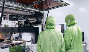
PrecisioNext, a leading domestic thermal compression bonding (TCB) equipment manufacturer, has officially launched its TCB laboratory.
NEW YORK, NEW YORK, UNITED STATES, September 30, 2025 /EINPresswire.com/ -- In response to the growing customer demand for advanced packaging technologies, PrecisioNext, a leading domestic thermal compression bonding (TCB) equipment manufacturer, has officially launched its TCB laboratory. The lab aims to offer end-to-end support spanning R&D, prototyping, and mass production, with a focus on four cutting-edge packaging areas:1. 2.5D Packaging: Including CoWoS-S and CoWoS-L packaging.
2. 3D Packaging: Such as multilayer DRAM chip stacking and bonding for HBM.
3. Co-Packaged Optics (CPO), oDSP, and Optical Module Packaging: Involving the heterogeneous integration of PIC (photonics IC)/EIC (electronics IC) with ASIC (application-specific integrated circuit), as well as oDSP (digital signal processor) for 1.6T optical modules. As chip sizes increase, traditional SMT and reflow processes are prone to warpage. TCB technology effectively addresses warpage issues in large chips.
4. Specialized Applications: Customized developments such as impact-resistant packaging for military/medical chips and low-temperature bonding.
TCB: A Key Solution to Break Through Advanced Packaging Bottlenecks
With the evolution of chip manufacturing processes and surging computational demands, high-end chips (e.g., GPU H100/H200, HBM, and oDSP) are trending toward larger sizes, higher I/O density, and smaller microbumps. Traditional flip-chip reflow processes face limitations in placement accuracy, warpage control, thermal drift, and voiding, leading to low yields and high failure rates—especially when bump pitch falls below 50µm or chip sizes increase.
Thermal compression bonding (TCB) addresses these challenges by using a localized bond head to apply precise heat (150–300°C) and pressure (10–200 MPa) to individual bumps. This process enables micron-level alignment and bonding within an inert gas chamber, with real-time monitoring of temperature-pressure-displacement curves. It also supports fluxless processes, creating reliable interconnections and emerging as a core solution to overcome advanced packaging bottlenecks.
Key benefits of TCB technology include:
1. High-Density Interconnect Capability: Supports up to 10,000 bumps per square millimeter (compared to ~2,000 for flip-chip), meeting the requirements of HBM multilayer DRAM stacking and 2.5D/3D packaging like CoWoS silicon interposers.
2. Warpage Suppression: Localized heating and coplanarity calibration (error < 3µm) resolve edge detachment issues in large chips (e.g., NVIDIA H-series > 800mm²) caused by CTE mismatch.
3. Process Flexibility: Compatible with various bonding materials such as TC-NCF and MR-MUF, adapting to diverse scenarios.
4. Support for Advanced Processes: Enables fluxless bonding for next-generation HBM4 and paves the way for sub-3µm bump pitches.
Loong Series TCB Equipment Empowers Domestic Chip Breakthroughs
With the booming demand for AI chips and HBM (the TCB equipment market is projected to reach $1.5 billion by 2027), traditional reflow processes can no longer support the continuation of Moore’s Law due to accuracy and yield limitations. TCB, with its localized thermal pressure control enabling micron-level interconnects, has become essential for HBM stacking and high-performance chip packaging.
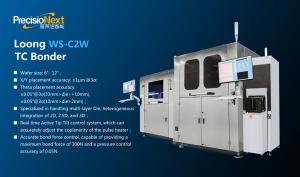
PrecisioNext’s Loong series breaks international monopolies, and its open laboratory provides rapid prototyping channels for CoWoS, CPO, and specialized fields, serving as a critical pivot for domestic advanced packaging development. As HBM layer counts increase to 16+ and bump diameters continue to shrink, TCB technical barriers will rise accordingly. The maturation of domestic equipment will accelerate the restructuring of the local supply chain’s influence.
Jack Li
Dongguan Precision Intelligent Technology Co., LTD
+86-13825438413
email us here
Visit us on social media:
Facebook
YouTube
Legal Disclaimer:
EIN Presswire provides this news content "as is" without warranty of any kind. We do not accept any responsibility or liability for the accuracy, content, images, videos, licenses, completeness, legality, or reliability of the information contained in this article. If you have any complaints or copyright issues related to this article, kindly contact the author above.


